
With projection micro stereolithography, HRL Laboratories pushes the limits of small size and intricate detail in additively manufactured interposers for 3D integration of microelectronic devices. © Getty Images.
With Micro Stereolithography, HRL Laboratories Pushes the Limits of Size and Detail in Additively Manufactured Packaging for Integrating Microelectronic Devices
HRL Laboratories, LLC’s additive manufacturing team has demonstrated 3D-printed interposers with previously impossible slanted and curved vias with diameters of less than 10µm. Vias are small openings in insulating layers of integrated circuits that allow conductive connections.
With conventional semiconductor processing methods like chemical etching, only straight vias can be fabricated. HRL is now 3D printing vias in polymer and ceramic materials with 2 µm resolution, allowing for complex routing. The vias are then metallized to electrically connect different devices and integrated circuits.
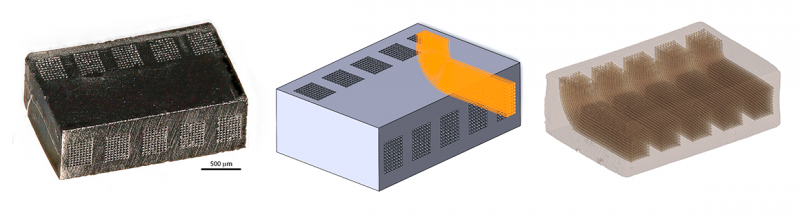
(Left) 3D printed ceramic part. (Center) Computer Aided Design of part with curved vias. (Right) Micro x-ray computer tomography image of curved vias in ceramic. © HRL Laboratories.
“We have printed arrays of straight and curved vias with an aspect ratio of at least 200:1. There is still room to increase this ratio using the low-viscosity preceramic resin that we developed in house,” said HRL Lead Engineer Kayleigh Porter.
In collaboration with Boston Micro Fabrication (BMF), HRL developed a print process for polymer-derived ceramics on BMF’s ultra-high-resolution, high-throughput Projection Micro Stereolithography 3D printer. The ability to print dielectric ceramics with temperature stability and durability is of high interest for microelectronic packaging applications.
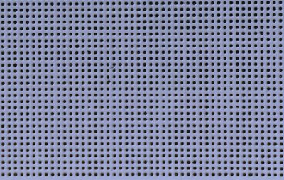
3D printed via array with 10um holes spaced at 20um pitch in ceramic. © HRL Laboratories.
“We are developing this technology to improve 3D integration of microelectronic subsystems such as infrared cameras and radar receivers,” said HRL group manager Dr. Tobias Schaedler. “Smaller, lighter, and more power-efficient system designs are currently limited by electrical routing and packaging, but our additive technology could resolve this bottleneck.”
HRL Laboratories’ development effort is currently funded by DARPA’s Microsystems Technology Office under the Focal arrays for Curved Infrared Imagers (FOCII) program.
This material is based upon work supported by the (DARPA) Defense Advanced Research Projects Agency under Contract No. N66001-20-C-4012. Any opinions, findings and conclusions or recommendations expressed in this material are those of the author(s) and do not necessarily reflect the views of the DARPA.
HRL Laboratories, LLC, California (hrl.com) pioneers the next frontiers of physical and information science. Delivering transformative technologies in automotive,aerospace and defense, HRL advances the critical missions of its customers. As a private company owned jointly by Boeing and GM, HRL is a source of innovations that advance the state of the art in profound and far-reaching ways.
Media Inquiries: media[at]hrl.com, (310) 317-5000